- 您现在的位置:买卖IC网 > Sheet目录1222 > ISL6521EVAL1 (Intersil)EVALUATION BOARD 1 ISL6521
�� �
�
�Application� Note� 1247�
�room� temperature� at� thermal� equilibrium� with� no� air� flow.� The�
�PWM� converter� design� targets� applications� which� specify� a�
�minimum� full� load� efficiency� of� 80%.� Design� modifications� to�
�the� output� inductor� and/or� dual� N-channel� MOSFETs� allow�
�for� achieving� higher� efficiency.�
�Adapting� Circuit� Performance�
�The� board� outlined� in� this� application� note� supports� the� use�
�of� both� surface� mount� and� thru� hole� devices.� This� feature�
�adds� flexibility� to� the� evaluation� process� by� allowing� easy�
�replacement� of� components� with� counterparts� for� cost�
�versus� performance� curve� balancing.�
�In� surface� mount� only� applications� or� designs� with� height�
�restrictions,� the� aluminum� electrolytic� bulk� output� capacitors�
�could� be� replaced� with� surface� mount� capacitors� with� similar�
�ESR� characteristics� and� achieve� similar� performance.� The�
�Sanyo� SVPC� series� or� Panasonic� SP� series� capacitors�
�provide� surface� mount� options� over� a� range� of� price� points.�
�Depending� on� the� PWM� output� voltage� ripple� requirements,�
�inductor� and� output� capacitor� selection� are� critical� in�
�achieving� desired� circuit� performance.� Care� must� be� taken�
�to� adjust� the� compensation� components� when� changing�
�output� capacitance� and/or� inductance.�
�Linear� Combinations�
�The� ISL6521� linear� controllers� can� be� used� individually� to�
�provide� 120mA� each� or� drive� an� external� pass� device� to�
�achieve� up� to� 3A.� Two� linear� controllers� can� be� ganged�
�together� to� create� one� 240mA� regulator� or� all� three� linears�
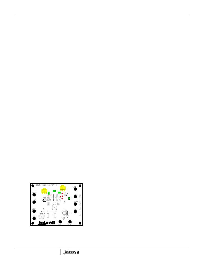
�can� be� tied� together� to� source� 360mA.� The� ISL6521EVAL1�
�evaluation� platform� supports� evaluation� of� this� option.� First,�
�the� external� pass� devices,� Q2� and� Q3,� must� be� removed.�
�The� external� pass� devices,� outlined� in� yellow,� are� highlighted�
�in� Figure� 9.� Next,� resistors� options,� outlined� in� green,� must�
�be� populated� to� short� the� output� planes� of� each� linear�
�together.� The� feedback� resistor� pairs,� accented� in� red,� for�
�each� linear� must� be� matching� to� provide� proper� voltage�
�feedback.� The� minimum� current� output,� over� temperature�
�Layout� Considerations�
�Component� placement� and� trace� layout� is� important� in� high�
�frequency� switching� converter� design.� With� power� devices�
�switching� efficiently� at� 300kHz,� the� resulting� current�
�transitions� from� one� device� to� another� cause� voltage� spikes�
�across� the� interconnecting� impedances� and� parasitic� circuit�
�elements.� These� voltage� spikes� can� degrade� efficiency,�
�radiate� noise� into� the� circuit,� and� lead� to� device� over-voltage�
�stress.� Careful� component� layout� and� printed� circuit� board�
�design� minimizes� these� voltage� spikes.�
�Component� Placement�
�The� switching� components� should� be� placed� close� to� the�
�ISL6521� first.� Minimize� the� length� of� the� connections� between�
�the� input� capacitors,� C4� and� C5,� and� the� power� switch,� Q1,� by�
�placing� them� nearby.� Position� both� the� ceramic� and� bulk� input�
�capacitors� as� close� to� the� upper� MOSFET� drain� as� possible.�
�Position� the� output� inductor� and� output� capacitors� between�
�the� upper� and� lower� MOSFETs� and� the� load.�
�The� critical� small� signal� components� include� any� bypass�
�capacitors,� feedback� components,� and� compensation�
�components.� Place� the� PWM� converter� compensation�
�components� close� to� the� FB� and� COMP� pins.� The� feedback�
�resistors� should� be� located� as� close� as� possible� to� the� FB�
�pin� with� vias� tied� straight� to� the� ground� plane� as� required.�
�Trace� Routing� and� Interconnects�
�Keep� the� trace� from� the� PHASE� terminal� to� the� output�
�inductor� short� and� wide.� A� power� plane� layer,� if� available,�
�should� support� the� input� power� and� output� power� nodes.�
�Use� copper� filled� polygons� on� the� phase� node� layers.� Keep�
�the� traces� from� the� UGATE� and� LGATE� pins� to� the� MOSFET�
�gates� short� and� wide� to� easily� handle� the� 1A� of� drive� current.�
�In� order� to� dissipate� heat� generated� by� the� internal� linears�
�and� PWM� drivers,� the� ground� pads� (pins� 5� and� 9)� should� be�
�connected� to� the� ground� plane� through� at� least� four� vias.�
�This� allows� the� heat� to� move� away� from� the� IC� and� also� ties�
�the� pad� to� the� ground� plane� through� a� low� impedance� path.�
�and� process� variations,� from� the� combined� linears� is� 300mA.�
�Summary�
�The� ISL6521EVAL1� is� an� adaptable� evaluation� tool� which�
�showcases� the� performance� of� the� ISL6521CB.� Designed� to�
�meet� the� performance� requirements� of� current� FPGA�
�applications,� it� allows� the� user� the� flexibility� to� configure� it� for�
�future� designs� as� well.� The� following� pages� provide� a�
�schematic� of� the� board,� bill� of� materials,� and� layout� drawings�
�to� support� implementation� of� this� solution.�
�References�
�Intersil� documents� are� available� on� the� web� at�
�FIGURE� 9.� COMPONENT� CHANGES� FOR� COMBINING�
�LINEARS�
�4�
�http://www.intersil.com/�
�[1]� ISL6521� Data� Sheet,� Intersil� Corporation,� File� No.�
�FN9148�
�AN1247.0�
�July� 10,� 2006�
�发布紧急采购,3分钟左右您将得到回复。
相关PDF资料
ISL6531EVAL2
EVALUATION BOARD 2 ISL6531
ISL6700EVAL1Z
EVALUATION BOARD FOR ISL6700
ISL6844EVAL1
EVALUATION BOARD 1 ISL6844
ISL6AHPEVAL1
EVAL BOARD HIP1011D/ISL6118
ISL70218SRHMEVAL1Z
EVALUATION BOARD FOR ISL70218SRH
ISL8107EVAL1Z
EVAL BOARD FOR ISL8107
ISL88550AEVAL1
EVALUATION BOARD 1 ISL88550A
ISL88694EVAL
EVALUATION BOARD ISL88694
相关代理商/技术参数
ISL6521EVAL1Z
功能描述:EVALUATION BOARD 1 ISL6521 RoHS:是 类别:编程器,开发系统 >> 评估板 - DC/DC 与 AC/DC(离线)SMPS 系列:- 产品培训模块:Obsolescence Mitigation Program 标准包装:1 系列:True Shutdown™ 主要目的:DC/DC,步升 输出及类型:1,非隔离 功率 - 输出:- 输出电压:- 电流 - 输出:1A 输入电压:2.5 V ~ 5.5 V 稳压器拓扑结构:升压 频率 - 开关:3MHz 板类型:完全填充 已供物品:板 已用 IC / 零件:MAX8969
ISL6521IBZ
功能描述:电压模式 PWM 控制器 4 IN 1 PWM/LINEAR CNTRLR 5V RoHS:否 制造商:Texas Instruments 输出端数量:1 拓扑结构:Buck 输出电压:34 V 输出电流: 开关频率: 工作电源电压:4.5 V to 5.5 V 电源电流:600 uA 最大工作温度:+ 125 C 最小工作温度:- 40 C 封装 / 箱体:WSON-8 封装:Reel
ISL6521IBZ-T
功能描述:电压模式 PWM 控制器 4 IN 1 PWM/LINEAR CNTRLR 5V RoHS:否 制造商:Texas Instruments 输出端数量:1 拓扑结构:Buck 输出电压:34 V 输出电流: 开关频率: 工作电源电压:4.5 V to 5.5 V 电源电流:600 uA 最大工作温度:+ 125 C 最小工作温度:- 40 C 封装 / 箱体:WSON-8 封装:Reel
ISL6522ACB
功能描述:IC REG CTRLR BST PWM VM 14-SOIC RoHS:否 类别:集成电路 (IC) >> PMIC - 稳压器 - DC DC 切换控制器 系列:- 标准包装:4,000 系列:- PWM 型:电压模式 输出数:1 频率 - 最大:1.5MHz 占空比:66.7% 电源电压:4.75 V ~ 5.25 V 降压:是 升压:无 回扫:无 反相:无 倍增器:无 除法器:无 Cuk:无 隔离:无 工作温度:-40°C ~ 85°C 封装/外壳:40-VFQFN 裸露焊盘 包装:带卷 (TR)
ISL6522ACB-T
功能描述:IC REG CTRLR BST PWM VM 14-SOIC RoHS:否 类别:集成电路 (IC) >> PMIC - 稳压器 - DC DC 切换控制器 系列:- 标准包装:4,000 系列:- PWM 型:电压模式 输出数:1 频率 - 最大:1.5MHz 占空比:66.7% 电源电压:4.75 V ~ 5.25 V 降压:是 升压:无 回扫:无 反相:无 倍增器:无 除法器:无 Cuk:无 隔离:无 工作温度:-40°C ~ 85°C 封装/外壳:40-VFQFN 裸露焊盘 包装:带卷 (TR)
ISL6522ACR
功能描述:IC REG CTRLR BST PWM VM 16-QFN RoHS:否 类别:集成电路 (IC) >> PMIC - 稳压器 - DC DC 切换控制器 系列:- 标准包装:4,000 系列:- PWM 型:电压模式 输出数:1 频率 - 最大:1.5MHz 占空比:66.7% 电源电压:4.75 V ~ 5.25 V 降压:是 升压:无 回扫:无 反相:无 倍增器:无 除法器:无 Cuk:无 隔离:无 工作温度:-40°C ~ 85°C 封装/外壳:40-VFQFN 裸露焊盘 包装:带卷 (TR)
ISL6522ACR-T
功能描述:IC REG CTRLR BST PWM VM 16-QFN RoHS:否 类别:集成电路 (IC) >> PMIC - 稳压器 - DC DC 切换控制器 系列:- 标准包装:4,000 系列:- PWM 型:电压模式 输出数:1 频率 - 最大:1.5MHz 占空比:66.7% 电源电压:4.75 V ~ 5.25 V 降压:是 升压:无 回扫:无 反相:无 倍增器:无 除法器:无 Cuk:无 隔离:无 工作温度:-40°C ~ 85°C 封装/外壳:40-VFQFN 裸露焊盘 包装:带卷 (TR)
ISL6522BCB
功能描述:IC REG CTRLR BST PWM VM 14-SOIC RoHS:否 类别:集成电路 (IC) >> PMIC - 稳压器 - DC DC 切换控制器 系列:- 标准包装:4,000 系列:- PWM 型:电压模式 输出数:1 频率 - 最大:1.5MHz 占空比:66.7% 电源电压:4.75 V ~ 5.25 V 降压:是 升压:无 回扫:无 反相:无 倍增器:无 除法器:无 Cuk:无 隔离:无 工作温度:-40°C ~ 85°C 封装/外壳:40-VFQFN 裸露焊盘 包装:带卷 (TR)